
In the week of Oct 19-23, 2015, a unique training on Photonic Integrated Circuits is being held at Columbia University in New York City. The training is one-stop-shop and covers all the material systems, whether Silicon, InP-based, or Triplex (SiO2/Si3N4). The training is supported by a broad consortium of companies, is hands-on as well as in-depth. For more info, please click on one of the tabs below.
There is a rapidly growing momentum for Photonic Integrated Circuits (PICs). After having held great promise for a good while, PICs have now been breaking through in applications such as 100G and beyond for long-haul telecom as well as for short-reach datacom. And because of that breakthrough, PICs are now proving attractive for other applications as well, such as optical switching in the datacenter, interrogators in fiber-sensing, and key components in next-gen FTTH.
However, the question how to get started in PICs is not necessarily trivial. Starting your own in-house effort including a waferfab plus packaging is unaffordable for most of the players. And even if you want to leverage the growing ecosystem of providers in software, foundries, and packaging, then the question is still which parts to do yourself, which parts to outsouce, and how to find the best tools and to familiarize yourself with them.

The purpose of this week-long in-depth training is to get you quickly up the learning curve by introducing you to all of the aspects that are critical for producing integrated optical components. The training covers system level essentials, a detailed tutorial on integrated optic components, in-depth simulations as well as mask layout, available foundry services for all material systems, packaging services, and relevant business fundamentals such as building a business case or scaling to production.
The training is tutorial, in-depth, hands-on, and practical. At the same time, there is ample room for the training to be dynamic and to allow for interaction with other participants. In this way, you can learn from each other as well as become familiar with instructors and the various players in the PIC ecosystem. The training is supported by the following organizations:
- Prof. Keren Bergman, Columbia University, Prof. Jonathan Klamkin, University of California Santa Barbara, and Michael Hochberg, Director of Strategy and Architecture at Coriant Advanced Technology
- Simulation and Layout Software: Mentor Graphics, Lumerical Solutions, PhoeniX Software
- Foundry Services: CEA-LETI, VTT, IMEC, Oclaro, HHI, Smart Photonics, LioniX, AIM Photonics
- Packaging: Chiral Photonics, Technobis
- Full Design Services: Bright Photonics, VLC Photonics
The training is held at Columbia University in New York City which is both inspiring due to the excellent PIC work that is being conducted there as well as offers a great environment for any after hours dining or entertainment.
Space is limited so there is a maximum to the number of trainees that can be accepted. Advance registration is required and there is a registration fee. The fee covers the week long training, copies of training materials, lunches and other in class refreshments, and installation of software as well as licenses required for that week. Trainees are responsible for booking hotel accommodation and for bringing in their laptops which can then be used for the PIC design and layout. In case of interest, laptops can be made available for on-site rental. Software licenses that cover a longer time for trial and evaluation can be made available on request as well.
For any questions about the training or logistics, please contact Isobel Hoevers at isobel@7pennies.com or (917) 833-3589.
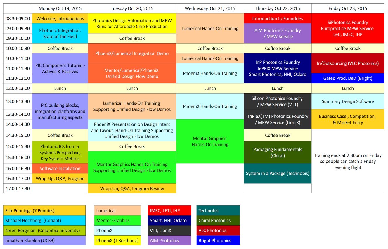
The week-long program is such that it provides a quick but in-depth training on everything that you need for producing photonic integrated components. The program covers system aspects, a component tutorial, simulations and chip layout, foundry services for all material systems, packaging, and Business/marketing essentials.
The schematic below shows the program for the week. “Please click on it for a magnified version.
Please click on the days below to get a detailed description of the program for that day.
Monday, October 19th 2015
09.00-10.00 | Photonic Integration: State of the Field (Michael Hochberg, Coriant)
10.00-10.30 | Coffee break
10.30-12.00 | PIC Component Tutorial – Actives & Passives (Jonathan Klamkin, UCSB)
12.00-13.00 | Lunch
13.00-14.30 | PIC building blocks, integration platforms and manufacturing aspects (Jonathan Klamkin, UCSB)
14.30-15.00 | Coffee break
15.00-16.00 | Photonic ICs from a Systems Perspective Overview of Key System Metrics (Keren Bergman, Columbia university)
16.00-16.30 | Software installation
16.30-17.00 | Wrap-Up, Q&A, Program
Tuesday, October 20th 2015
08.30-09.30 | Photonics Design Automation and MPW Runs for Affordable Chip Production (PhoeniX, T. Korthorst)
09.30-10.00 | Coffee break
10.00-11.00 | Integration Demo (PhoeniX, Lumerical)
11.00-12.00 | Unified Design Flow Demo (Mentor, Lumerical, PhoeniX)
12.00-13.00 | Lunch
13.00-14.00 | Hands-On Training Supporting Unified Design Flow Demos (Lumerical)
14.00-15.00 | Presentation on Design Intent and Layout. Hand-On Training Supporting Unified Design Flow Demos (PhoeniX)
15.00-15.30 | Coffee break
15.30-17.00 | Hands-On Training Supporting Unified Design Flow Demos (Mentor Graphics)
17.00-17.30 | Wrap-Up, Q&A, Program Review
Wednesday, October 21th 2015
08.30-10.00 | Lumerical Hands-On Training
10.00-10.30 | Coffee break
10.30-11.00 | Lumerical Hands-On Training
11.00-12.00 | PhoeniX Hands-On Training
12.00-13.00 | Lunch
13.00-14.00 | PhoeniX Hands-On Training
14.00-16.00 | Mentor Graphics Hands-On Training
Thursday, October 22th 2015
08.30-09.00 | Introduction to Foundries (CEA-LETI, IMEC, IHP)
09.00-10.00 | AIM Photonics Foundry / MPW Service
10.00-10.30 | Coffee break
10.30-12.00 | InP Photonics Foundry (JePPIX MPW Service Smart Photonics, HHI, Oclaro)
12.00-13.00 | Lunch
13.00-14.00 | Silicon Photonics Foundry / MPW Service (VTT)
14.00-14.30 | TriPleX(TM) Photonics Foundry / MPW Service (LioniX)
14.30-15.00 | Coffee break
15.00-16.00 | Packaging Fundamentals (Chiral)
16.00-17.00 | System in a Package (Technobis)
Friday, October 23th 2015
08.30-10.00 | SiPhotonics Foundry Europractice MPW Service (CEA-LETI, IMEC, IHP)
10.00-10.30 | Coffee break
10.30-11.30 | In/outsourcing (VLC Photonics)
11.30-12.00 | Gated product development (Bright Photonics)
12.00-13.00 | Lunch
13.00-13.30 | Summary Design Software (PhoeniX)
13.30-14.30 | Business Case, Competition, & Market Entry (Erik Pennings)
Training ends at 2:30pm on Friday so people can catch a Friday evening flight
For any questions about the training or logistics, please contact Isobel Hoevers at isobel@7pennies.com or (917) 833-3589.
The training is supported by a wide group of service providers to the PIC industry. It includes foundries for pretty much all the relevant material systems, providers of simulation and layout software, packaging houses, as well as providers of turn-key PIC design solutions. The common denominator for all these companies is that they support multi-project wafer (MPW) runs, which are a great and cost-effective way to develop PICs. For a description of all the sponsors, please see the relevant sections below.

Imec performs world-leading research in nanoelectronics. We leverage our scientific knowledge with the innovative power of our global partnerships in ICT, healthcare and energy. We deliver industry-relevant technology solutions. In a unique high-tech environment, our international top-talent is committed to providing the building blocks for a better life in a sustainable environment.

Europractice was launched by the European Commission in October 1995 to help companies improve their competitive position in world markets by adopting ASIC, Multi-Chip Module (MCM) or Microsystems solutions in the products they manufacture. The program helps to reduce the perceived risks and costs associated with these technologies by offering potential users a range of services, including initial advice and ongoing support, reduced entry costs and a clear route to chip manufacture and product supply.

VTT Technical Research Centre of Finland Ltd engages in applied technology research, transforming its research results into practical solutions. VTT Ltd uses its research and knowledge to provide expert services for its domestic and international customers and partners in both the private and public sector. VTT Ltd is Finland’s biggest applied research organisation and the Nordic countries’ leading research and technology company. As one of the first pioneers in the field, VTT has developed it’s silicon photonics technology since 1997. Its micron-scale SOI technology has been offered through MPW runs (ePIXfab) since 2014. Now the 3 µm SOI platform is expanding from passive and thermo-optic circuits to high-speed active components in close collaboration with industrial customers and partners. (https://www.vtt.fi/siliconphotonics)

JePPIX is a broker that helps organizations around the globe to get access to advanced fabrication processes for Photonic Integrated Circuits (PICs). JePPIX aims at low-cost development of application specific PICs using a generic foundry model and rapid prototyping via industrial Multi-Project Wafer runs. The generic approach allows a variety of PICs to be realized using the same standardized processes. JePPIX closely collaborates with Europe’s key players in the field of photonic integration, including manufacturing and packaging partners, photonic CAD software partners, R&D labs and photonic IC design houses. With JePPIX you can get access to the Indium Phosphide (InP)-based monolithic integration platforms of Oclaro, Fraunhofer HHI and SMART Photonics and the low-loss dielectric TriPleX waveguide technology of LioniX. JePPIX is hosted by the Eindhoven University of Technology in the Netherlands. For more information visit our website: (www.jeppix.eu).

Fraunhofer HHI The core competencies of Fraunhofer HHI are in the areas of Photonic Networks and Systems, Mobile Broadband Systems, Photonic Components and Electronic Imaging. Within the Fraunhofer mission “to undertake applied research of direct utility to private and public enterprise and of wide benefit to society”, we offer research, development and production services in all our activities to the German and international industry. The activities of the Photonic Components Dept. are focused on the following – mainly InP based- optical components for tele- and datacom, and optical sensing applications. Components such as: Photonic Integrated Circuits, Integrated hybrid InP and Polymer PLC components, THz Components, Discrete devices, DOE and related devices, InP MOVPE; e-beam lithography; process development; & Qualification support. (www.hhi.fraunhofer.de)

SMART Photonics, located in Eindhoven, The Netherlands, is a Pure Play Foundry offering III-V production services for both discrete- as well as integrated- Indium Phosphide based photonic components. We use our knowledge, experience and the dedicated equipment to create and produce the photonic designs of our customers. We offer the complete production process from Epitaxial growth, processing, re-growth and polishing of wafers up to dicing and coating of the sides of the chips. Next to the production support, in either the proof of concept (POC) phase or the full production phase, we also offer single- or combined- process steps to complete, or back-up, the production processes of our customers. (www.smartphotonics.nl)

LioniX is a leading provider in development and small to high volume production of leveraging and innovative products based on micro/nano system technology (MNT) and MEMS. Our core technologies are integrated optics and micro-fluidics. Our customers operate in telecom, industrial process control, life sciences and space markets and include OEM’s, multinationals, VC start-up companies as well as research institutions from around the world. LioniX offers design to manufacturing and horizontal integration by partnering with MEMS/MST foundries and suppliers of complementary technologies, such as in (food) biotech/genomics, chemistry/pharmaceuticals and water technology. The combination of micro-fluidics and their integrated optics technology (TriPleX™) gives LioniX an unrivalled expertise in the emerging area of Lab-on-a-Chip. (www.lionixbv.nl)

Lumerical-Since its inception in 2003, Lumerical has pioneered breakthrough simulation technologies that help bring new photonic product concepts to life. By empowering research and product development professionals with high performance photonic design software that leverages recent advances in computing technology, Lumerical helps optical designers tackle challenging design goals and meet strict deadlines. Lumerical’s design software solutions have been licensed in more than 40 countries by global technology leaders like Samsung, STMicroelectronics, Huawei, Agilent, Olympus, and Philips, and prominent research institutions including Caltech, Harvard, Max Planck Institute, MIT, NIST, University of Tokyo and the Chinese Academy of Sciences. Discover how Lumerical can help you meet your own design objectives. (www.lumerical.com)

Mentor Graphics – Building an EDA Environment for Silicon Photonics: Silicon photonics has a huge potential for signal processing applications ranging from communications to biosensors and opto-MEMS devices. However, the expansion of available photonic components is currently limited by the large amount of engineering effort required to accurately design known reliable components in a system. Mentor Graphics, a leading supplier in the Electronics Design Automation industry, is working to extend the tools and best practices that have enabled the rapid design of high-volume CMOS application-specific integrated circuits to the silicon photonics design community. (www.mentor.com)

PhoeniX Software, Based on a history going back to 1991, provides an unique mask lay-out, process flow design and simulation environment for the integrated photonics marketplace. Headquartered in Enschede, the Netherlands, PhoeniX Software supports customers around the globe through its subsidiaries and network of sales representatives to improve quality, reduce time to market and enhance research by offering unique and highly integrated software solutions, training and customer support. Customers range from Fortune 500 companies to start-ups, universities and research institutes, active in integrated photonics, microfluidics, MEMS, printed electronics and other micro and nano technologies. Furthermore PhoeniX Software is supporting Multi Project Wafer runs at various foundries with dedicated PDKs for TriPleX, InP and silicon photonics. (https://www.phoenixbv.com)

Bright Photonics B.V. is a design house for photonic integrated circuits (PICs), also referred to as systems on chip (SoC). Our mission is to make PICs accessible to (small) businesses, research institutes and universities in technologies as SoI, InP, Triplex, glass and polymers. Bright Photonics operates as an intermediate company between foundry services and product developers. We are the commercial design partner in the two largest active European projects in the field of integrated photonics. Our strategy is to be your gateway to photonic ICs from application idea to PIC, at the level where you need it: feasibility, layout, access to multi-project wafer runs and/or packaged prototypes. In addition to design services, Bright Photonics can support you with fab-ready design libraries for photonic components such as AWG multiplexers. These are also adaptable to your custom process and needs. Contact Bright Photonics and find out what PICs can do for your product or research. (https://www.brightphotonics.eu/)

VLC Photonics aims to be a complete but flexible partner in photonic integration, thanks to its deep expertise in the whole integration process, from the preliminary feasibility studies, to fabrication platform selection, optical chip design, foundry and packager brokerage, and chip characterization and test. VLC Photonics has been working for more than 14 years in the field, with experience in all major international fabs (+15) in all main material substrates (silicon photonics, InP, GaAs, PLC, SiN, TriPleX, etc.). Our know-how includes multiple passive and active components like AWGs, MMIs, Echelle gratings, modulators, lasers, switches, filters, etc. Our field of expertise is mostly in optical telecommunications, datacom and optical interconnects, microwave photonics, quantum optics, and sensing systems like fiber sensor interrogators or biophotonics lab-on-a-chip. Check our website for more info and references, and an on-line pricing tool for multi-project wafer runs! (https://vlcphotonics.com)

Chiral Photonics (CPI), a New Jersey, US based company founded in 1999, specializes in optoelectronic packaging of integrated photonics. CPI offers its pitch reducing optical fiber arrays, PROFAs, which enable the highest density optical I/Os for both edge and face coupling to photonic ICs. Currently, up to 61 I/O channels can be coupled in a single port. Other services range from single-die optical coupling or optoelectronic package development, including test services, to volume optoelectronic production packaging.Please contact us to obtain our free coupling and packaging design guidelines: designguide@chiralhotonics.com.

Technobis Fibre Technologies is specialized in the development and supply of fibre optic sensing systems and applications. All developments are spectrometry and or interferometry based. Optical fibre sensors find widespread use for a multitude of applications due to their small size, light weight, inertness to chemical substances, ability to withstand high temperatures and immunity for electromagnetic interference. Subsequently, optical fibre sensors are frequently used for applications such as Structural Health Monitoring (SHM), where the deformation and dynamic response behavior of objects are measured using mounted or even embedded optical fibers to the structure being monitored. All new developments are based on integrated photonics. Application Specific Photonic Integrated Circuits (ASPIC) are optical chips designed for dedicated purposes. Similar to electronics, ASPICs allows a versatility of solutions, all based on a small set of components providing improved performances and reliability. The versatile ability to replace traditional assemblies of multiple discrete optical or micro-optical components by a single small sized chip, make ASPICs highly favorable for next generation optical systems for benefits in cost reduction, functionality aggregation and standardization of specifications and processes. (www.technobis.com)

Oclaro, Inc. (Nasdaq: OCLR), is a leader in optical components, modules and subsystems for the core optical, enterprise and data center, and wireless access markets. Leveraging more than three decades of laser technology innovation, photonic integration, transceiver and subsystem design, Oclaro’s solutions are at the heart of the fast optical networks and high-speed interconnects driving the next wave of streaming video, cloud computing, voice over IP, SaaS and other high-speed and bandwidth-intensive applications. (www.oclaro.com)

CEA (Commissariat à l’Energie Atomique et aux Energies Alternatives) is a French Governmental Research Organization (15,000 employees). Within the “CEA-TECH” branch devoted to industrial Research & Development, CEA-LETI is one of the major European research centers in applied electronics, optics and sensing. It is located in Grenoble-France where it operates 11,000 m²-State-of-the-Art CMOS clean rooms (200 and 300 mm wafer size), and a MEMS microsystems platform (200 mm wafer size). Nearly 1,600 men and women are serving innovation and the transfer of technology in key domains. Besides, CEA-LETI has sparked the creation of thirty high-technology start-ups, including Soitec, world leader in the development/ production of Silicon on insulator wafers.
As a pioneer in Research & Development in Silicon Photonics (since 2002), CEA-LETI has developed strong expertise and know how in the design, fabrication and test of integrated devices (including Ge-on-Silicon photodetectors and hybrid III/V-on-Silicon lasers) and circuits for telecom and datacom applications. ST microelectronics is one of its main industrial partner in the field.

IHP has a team of 300 R&D professionals with core competence in micro-electronics: process technology, circuit design, and systems. As a member institute of the Gottfried Wilhelm Leibniz Society, the core funding comes from the German Federal Government and the State Government of Brandenburg.
IHP is an established international foundry and development partner for companies and academic partners in the area of silicon photonics, or, more specifically photonic-electronic integration. For several years we have been developing monolithic photonic electronic integration technology based on high-performance BiCMOS technology featuring ~200GHz transistors. All silicon photonics technologies and prototypes are developed and fabricated in our cleanroom facility housing a 200mm BiCMOS toolset including DUV lithography. In the frame of ePIXfab and EUROPRACTICE photonic integrated circuit technologies are being offered in multi-project wafer runs. IHP’s photonic BiCMOS technology is a strategic asset for IHP’s integrated approach from technology to systems to provide a portfolio of enabling photonic sub-system and system solutions.
Sponsor / Host

At Columbia’s Electrical Engineering Department we are continuing to push forward the frontiers of what can be done with devices, circuits, systems, signals, and information. Our department combines top-tier research with a rigorous and vibrant learning environment for all our students, and we are proud of the balance we provide between the many aspects of EE — both theoretical and practical, and between traditional and emerging fields.
Association Supporter

EPIC is the industry association that promotes the sustainable development of organisations working in the field of photonics in Europe. We foster a vibrant photonics ecosystem by maintaining a strong network and acting as a catalyst and facilitator for technological and commercial advancement. EPIC publishes market and technology reports, organizes technical workshops and B2B roundtables, coordinates EU funding proposals, advocacy and lobbying, education and training activities, standards and roadmaps, pavilions at exhibitions. (www.epic-assoc.com)

The training is held at the Presidential Ballroom (Pres123R) of the Faculty House of Columbia University in New York City. This venue is inspiring due to the excellent PIC work that is being conducted at Columbia University. In addition, New York City offers a great environment for any after hours dining or entertainment. The address is:
- Columbia University, Faculty House
- 64 Morningside Drive
- New York, NY 10027
New York is well reachable via either the John F Kennedy (JFK), Laguardia (LGA) or Newark (EWR) airports. For Google directions to the EE dept, please click on the map below. And for a detailed map of the campus, please click here.

For any questions about the training or logistics, please contact Isobel Hoevers at isobel@7pennies.com or (917) 833-3589.

New York is a beautiful city and a popular travel destination, that offers a large amount of hotel accommodations. Given that the training starts early on Monday Oct 19, we recommend that you arrive on (or before) Sunday Oct 18. And on Friday Oct 23, the training ends at 2:30pm so as to allow participants to travel back home on Friday evening.
A great overview of recommended hotels as well as other practical information can be found on the website of Columbia University. For more information, click here.
For additional possibilities, pricing, and ratings, please check out Expedia with a listing of hotels around Columbia University.
PIC ARCHIVE
For more info, please check out the archived earlier photonic integration events. Material for these events has been posted and is available on request.