
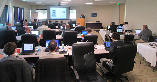
After two successful training events in 2015 and 2016 with very enthusiastic reactions, a third training is now organized, this time in Santa Clara, California. The training is one-stop-shop and covers all the material systems, whether Silicon, InP-based, or dielectrics such as TriPleX (SiO2/Si3N4). The training is supported by a broad consortium of companies and is hands-on as well as in-depth. For more info, please click on one of the tabs below.
There is a rapidly growing momentum for Photonic Integrated Circuits (PICs). After having held great promise for a good while, PICs have now been breaking through in applications such as 100G and beyond for long-haul telecom as well as for short-reach datacom. And because of that breakthrough, PICs are now proving attractive for other applications as well, such as optical switching in the datacenter, interrogators in fiber-sensing, and key components in next-gen FTTH. The fact that the PIC workshop that we recently organized at OFC 2017 attracted close to 380 people is evidence of this growing interest in photonic integration.
However, the question how to get started in PICs is not necessarily trivial. Starting your own in-house effort including a waferfab plus packaging is unaffordable for most of the players. And even if you want to leverage the growing ecosystem of providers in software, foundries, and packaging, then the question is still which parts to do yourself, which parts to outsource and how to find the best tools and familiarize yourself with them.
The purpose of this week-long in-depth training is to get you quickly up the learning curve by introducing you to all of the aspects that are critical for producing integrated optical components. The training covers system level essentials, a detailed tutorial on integrated optic components, in-depth simulations as well as mask layout, available foundry services for all material systems, packaging services, test & measurement and relevant business fundamentals such as building a business case or scaling to production.
The PIC training provides the ideal orientation for managers or engineers in companies that want to start in photonic integration or who feel that PICs are becoming increasingly important. The training is also very useful for any new employees or graduate students who are active in photonic integration and who need a better understanding of PIC technology, tools, as well as the full value chain. And the PIC training is valuable for anyone who needs to make a decision about which design software to acquire or which material system or foundry to use.
Space is limited so there is a maximum to the number of trainees that can be accepted. Advance registration is required and there is a registration fee. The fee covers the week long training, copies of training materials, lunches and other in class refreshments, and installation of software as well as licenses required for that week. Trainees are responsible for booking hotel accommodation and for bringing in their laptops which can then be used for the PIC design and layout. In case of interest, laptops can be made available for on-site rental. Software licenses that cover a longer time for trial and evaluation can be made available on request as well.
For any questions about the training or logistics, please contact Erik Pennings at erik@7pennies.com or (848) 228-0807.
Testimonials
Please see below for a number of reactions from the previous training events that were held at Columbia University in Oct 2015 and in Silicon Valley in Nov 2016:
“Overall, it was a great selection of speakers. I appreciate the comprehensive topic coverage.”
“Organization of event was excellent liked distribution of all contact info and multiple updates up to the start of the training.”
“I really appreciated this training. All was perfect; content, organization, supports…”
“Thanks a lot! … and thanks again for the PIC training – it was very helpful to me.”
“This was done well. Better then most workshops I have attended…”
“Excellent location, venue, catering etc.!”
“I liked the software tutorials and the talks about the current state of the art and future trends of PIC’s.”
“Networking very good. I talked to a lot of experts in the field.”
“All excellent speakers, all of them knew their content well, and were very approachable…” “Excellent organization… I can’t think of anything that could be improved…”
“Excellent networking, excellent people, excellent chances to network during the breaks. A lot of thanks … for organizing all the dinners in the evening – which allowed more deeper networking opportunities.”
“I liked the program very much. Covered all the essential steps in a PIC packaging cycle…”
The week-long program is such that it provides a quick but in-depth training on everything that you need for producing photonic integrated circuits. The program covers system aspects, a component tutorial, simulations and chip layout, foundry services for all material systems, packaging, test & measurement, and business/marketing essentials.
The schematic below shows the preliminary training program for the week. Please click on the schedule for a magnified version. The schedule below will be updated as soon as additional detail becomes available.
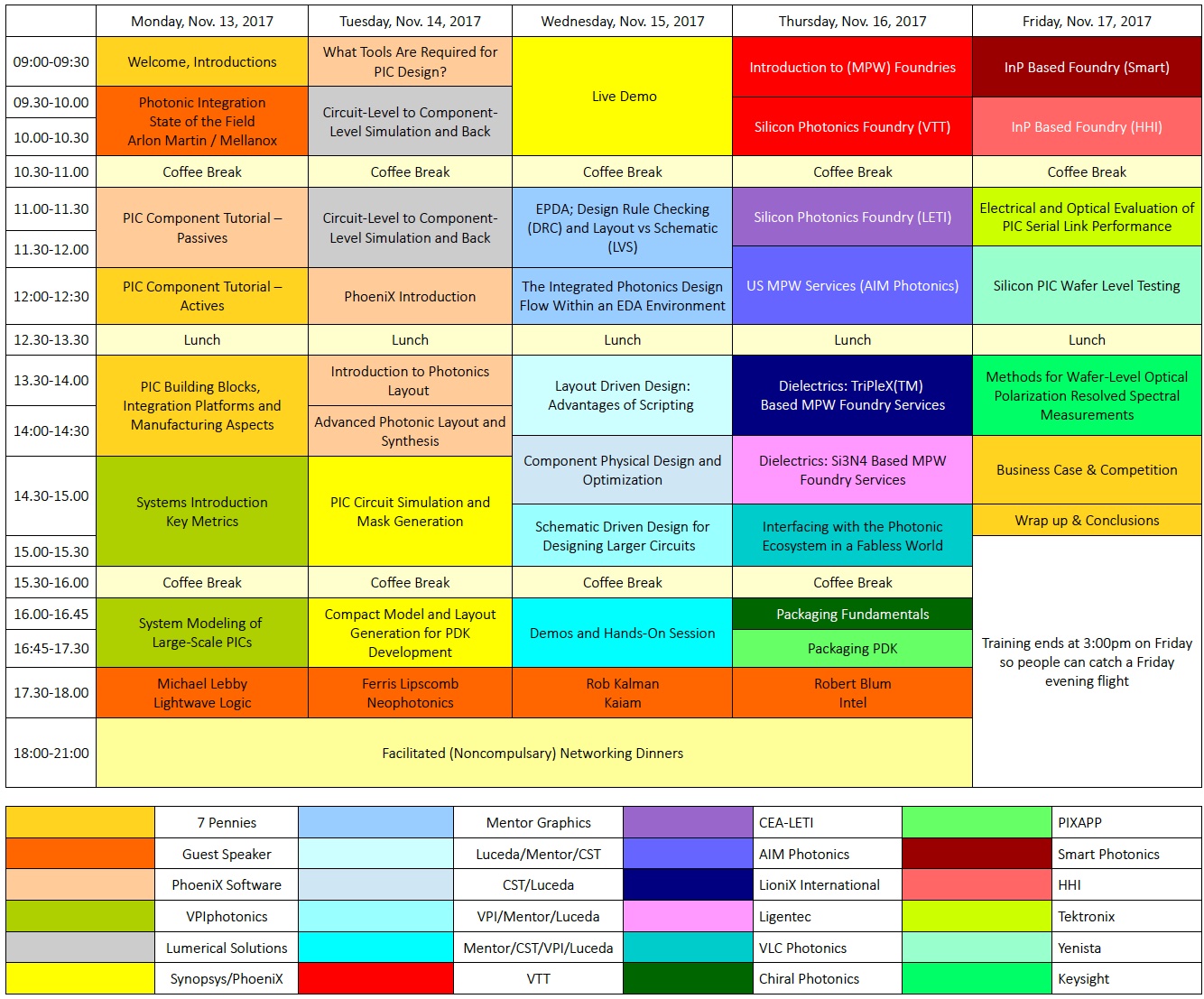
Please click on the days below to get a detailed description of the program for that day.
Monday November 13th
09.00-09.30 | Welcome, Introductions
09.30-10.30 | Photonic Integration State of the Field Arlon Martin / Mellanox
10.30-11.00 | Coffee break
11.00-12.00 | PIC Component Tutorial – Passives
12.00-12.30 | PIC Component Tutorial Actives
12.30-13.30 | Lunch
13.30-14.30 | PIC building blocks, integration Platforms and Manufacturing Aspects
14.30-15.30 | Systems Introduction Key Metrics
15.30-16.00 | Coffee break
16.00-17.30 | System Modeling of Large-Scale PICs
17.30-18.00 | Michael Lebby Lightwave Logic
18.00-21.00 | Facilitated (Noncompulsary) Networking Dinners
Tuesday November 14th
09.00-09.30 | What Tools Are Required for PIC Design?
09.30-10.30 | Circuit-Level to Component- Level Simulation and Back
10.30-11.00 | Coffee break
11.00-12.00 | Circuit-Level to Component- Level Simulation and Back
12.00-12.30 | PhoeniX Introduction
12.30-13.30 | Lunch
13.30-14.00 | Introduction to Photonics Layout
14.00-14.30 | Advanced Photonic Layout and Synthesis
14.30-15.30 | PIC Circuit Simulation and Mask Generation
15.30-16.00 | Coffee break
16.00-17.30 | Compact Model and Layout Generation for PDK Development
17.30-18.00 | Ferris Lipscomb Neophotonics
18.00-21.00 | Facilitated (Noncompulsary) Networking Dinners
Wednesday November 15th
09.00-10.30 | Live Demo
10.30-11.00 | Coffee break
11.00-12.00 | EPDA; Design Rule Checking (DRC) and Layout vs Schematic (LVS)
12.00-12.30 | The Integrated Photonics Design Flow Within an EDA Environment
12.30-13.30 | Lunch
13.30-14.15 | Layout Driven Design: Advantages of Scripting
14.15-14.45 | Component Physical Design and Optimization
14.15-15.30 | Schematic Driven Design for Designing Larger Circuits
15.30-16.00 | Coffee break
16.00-17.30 | Demos and Hands-On Session
17.30-18.00 | Rob Kalman Kaiam
18.00-21.00 | Facilitated (Noncompulsary) Networking Dinners
Thursday November 16th
09.00-09.45 | Introduction to (MPW) Foundries
09.45-10.30 | Silicon Photonics Foundry (VTT)
10.30-11.00 | Coffee break
11.00-11.45 | Silicon Photonics Foundry (LETI)
11.45-12.30 | US MPW Services (AIM Photonics)
12.30-13.30 | Lunch
13.30-14.15 | Dielectrics: TriPleX(TM)Based MPW Foundry Services
14.15-14.45 | Dielectrics: Si3N4 Based MPW Foundry Services
14.45-15.30 | Interfacing with the Photonic Ecosystem in a Fabless World
15.30-16.00 | Coffee break
16.00-16.10 | Optimize Your PIC Design Flow with Open Source, Python, Klayout and Nazca (Bright Photonics)
16:10-16:50 | Packaging Fundamentals (Chiral Photonics)
16.50-17.30 | Packaging PDK (PIXAPP)
17.30-18.00 | Robert Blum Intel
18.00-21.00 | Facilitated (Noncompulsary) Networking Dinners
Friday November 17th
09.00-09.45 | InP Based Foundry (Smart)
09.45-10.30 | InP Based Foundry (HHI)
10.30-11.00 | Coffee break
11.00-11.45 | Electrical and Optical Evaluation of PIC Serial Link Performance
11.45-12.30 | Silicon PIC Wafer Level Testing
12.30-13.30 | Lunch
13.30-14.00 | Methods for Wafer-Level Optical Polarization Resolved Spectral Measurements
14.00-14.15 | Business case & Competitiony
14.15-15.00 | Wrap up & Conclusions
Training ends at 3:00pm on Friday so people can catch a Friday evening flight
For any questions about the training or logistics, please contact Erik Pennings at erik@7pennies.com or (848) 228-0807.
The training will be supported by a wide group of service providers to the PIC industry. It includes foundries for pretty much all the relevant material systems, providers of simulation and layout software, packaging houses, as well as providers of turn-key PIC design solutions. Please see below the list of companies that are supporting the PIC training.

JePPIX is a broker that helps organizations around the globe to get access to advanced fabrication processes for Photonic Integrated Circuits (PICs). JePPIX aims at low-cost development of application specific PICs using a generic foundry model and rapid prototyping via industrial Multi-Project Wafer runs. The generic approach allows a variety of PICs to be realized using the same standardized processes. JePPIX closely collaborates with Europe’s key players in the field of photonic integration, including manufacturing and packaging partners, photonic CAD software partners, R&D labs and photonic IC design houses. With JePPIX you can get access to the Indium Phosphide (InP)-based monolithic integration platforms of Oclaro, Fraunhofer HHI and SMART Photonics and the low-loss dielectric TriPleX waveguide technology of LioniX. JePPIX is hosted by the Eindhoven University of Technology in the Netherlands. For more information visit our website: (www.jeppix.eu).

SMART Photonics, located in Eindhoven, The Netherlands, is a Pure Play Foundry offering III-V production services for both discrete- as well as integrated- Indium Phosphide based photonic components. We use our knowledge, experience and the dedicated equipment to create and produce the photonic designs of our customers. We offer the complete production process from Epitaxial growth, processing, re-growth and polishing of wafers up to dicing and coating of the sides of the chips. Next to the production support, in either the proof of concept (POC) phase or the full production phase, we also offer single- or combined- process steps to complete, or back-up, the production processes of our customers. (www.smartphotonics.nl)

Fraunhofer HHI The core competencies of Fraunhofer HHI are in the areas of Photonic Networks and Systems, Mobile Broadband Systems, Photonic Components and Electronic Imaging. Within the Fraunhofer mission “to undertake applied research of direct utility to private and public enterprise and of wide benefit to society”, we offer research, development and production services in all our activities to the German and international industry. The activities of the Photonic Components Dept. are focused on the following – mainly InP based- optical components for tele- and datacom, and optical sensing applications. Components such as: Photonic Integrated Circuits, Integrated hybrid InP and Polymer PLC components, THz Components, Discrete devices, DOE and related devices, InP MOVPE; e-beam lithography; process development; & Qualification support. (www.hhi.fraunhofer.de)

The American Institute for Manufacturing Integrated Photonics (AIM Photonics), is an industry driven public-private partnership that focuses the nation’s premiere capabilities and expertise to capture critical global manufacturing leadership in a technology that is both essential to National security and positioned to provide a compelling return-on-investment to the U.S. economy. The Institute’s goal is to emulate the dramatic successes experienced by the electronics industry over the past 40 years and transition key lessons, processes, and approaches to the photonic integrated circuit (PIC) industry. AIM Photonics supports Small and Medium Enterprises, providing practical access and technology on-ramps for U.S. industry, government, and academic communities. We are creating a National PIC manufacturing infrastructure, widely accessible and inherently flexible to meet the challenges of the marketplace with practical, innovative solutions. (www.aimphotonics.com)

LioniX International B.V. is a leading global provider of customized microsystem solutions, in particular integrated photonics-based, in scalable production volumes. We provide customized solutions for OEM’s and System Integrators, from design to device, by vertical integration in scalable production volumes and maintaining technology leadership secured by strong IP position. As LioniX International we focus on Photonic Integrated Circuits (PIC) enabled modules based on our proprietary waveguide technology (TriPleX™), in addition to our other core competences micro-fluidics, opto-fluidics and MEMS. As vertically integrated company we deliver a complete solution to our OEM customers: from initial design through volume manufacturing of products.
LioniX International B.V. has been established in April 2016, funded by Panthera Group B.V. and YMK Photonics Co., Ltd. LioniX International B.V. is a private company and has been established in April 2016, following the acquisition of SATRAX B.V., XiO Photonics B.V., LioniX B.V. and OctroliX B.V., which initiated the technology development of photonic integrated circuits for a suite of applications since 2001. Currently LioniX International employs nearly 50, highly educated people, and its management has experience in the micro/nano system technology for decades. (www.lionix-int.com)

ePIXfab is a European alliance of organizations that promotes silicon photonics science, technology, and application through a fabless model for the development of silicon photonic circuits based on existing photonics and CMOS infrastructure. (http://epixfab.eu)

CEA (Commissariat à l’Energie Atomique et aux Energies Alternatives) is a French Governmental Research Organization (15,000 employees). Within the “CEA-TECH” branch devoted to industrial Research & Development, CEA-LETI is one of the major European research centers in applied electronics, optics and sensing. It is located in Grenoble-France where it operates 11,000 m²-State-of-the-Art CMOS clean rooms (200 and 300 mm wafer size), and a MEMS microsystems platform (200 mm wafer size). Nearly 1,600 men and women are serving innovation and the transfer of technology in key domains. Besides, CEA-LETI has sparked the creation of thirty high-technology start-ups, including Soitec, world leader in the development/ production of Silicon on insulator wafers.
As a pioneer in Research & Development in Silicon Photonics (since 2002), CEA-LETI has developed strong expertise and know how in the design, fabrication and test of integrated devices (including Ge-on-Silicon photodetectors and hybrid III/V-on-Silicon lasers) and circuits for telecom and datacom applications. ST microelectronics is one of its main industrial partner in the field. (http://www.cea.fr/english/Pages/cea/the-cea-a-key-player-in-technological-research.aspx)

VTT Technical Research Centre of Finland Ltd engages in applied technology research, transforming its research results into practical solutions. VTT Ltd uses its research and knowledge to provide expert services for its domestic and international customers and partners in both the private and public sector. VTT Ltd is Finland’s biggest applied research organisation and the Nordic countries’ leading research and technology company. As one of the first pioneers in the field, VTT has developed it’s silicon photonics technology since 1997. Its micron-scale SOI technology has been offered through MPW runs (ePIXfab) since 2014. Now the 3 µm SOI platform is expanding from passive and thermo-optic circuits to high-speed active components in close collaboration with industrial customers and partners. (www.vtt.fi/siliconphotonics)

LIGENTEC is offering wafer scale fabrication of silicon nitride photonic integrated circuits (PIC) for applications in telecom/datacom, quantum optics, optical (bio-)sensing. The propriatory low loss waveguide technology together with the low bending losses that thick film nitride enables paves the way to new integrated applications. Thick silicon nitride chips can thus scale down to four times in cost compared to thin film silicon nitride. The combination of cost scaling and low loss is resulting in more cost-effective solutions. (https://www.ligentec.com)

Pioneering photonics design automation already since 1991, today PhoeniX Software has a global presence and is a trusted and well recognized partner for a large number of organizations. We enable easy and cost-effective realization of integrated photonics chips and systems, by means of our internally developed superior products and services. Our customers range from large OEM’s to start-ups and include some of the world’s top universities and research institutes. As the leader in Photonic IC design solutions, we will continue to develop the market by anticipating market demand and customer needs. In combination with our strategic partnerships, this results in offering world class design flows and access to all relevant fabrication technologies for our customers. (http://www.phoenixbv.com)

Lumerical – Since its inception in 2003, Lumerical has pioneered breakthrough simulation technologies that help bring new product concepts to life. Lumerical’s software tools support a broad range of photonic and electromagnetic design and analysis applications. From component level analysis using optical and electrical solvers to photonic integrated circuit and system design and simulation, Lumerical’s products are capable of addressing the most challenging design problems. Lumerical’s photonic design tools are licensed in nearly 50 countries, by more than 800 of the world’s most innovative organizations including 7 of the top 10 companies in the S&P 1200 Global IT Index and 44 of the top 50 research universities according to the Times Higher Education rankings. (www.lumerical.com)

VPIphotonics sets the industry standard for end-to-end photonic design automation comprising design, analysis and optimization of components, systems and networks. We provide professional simulation software supporting requirements of integrated photonics, optoelectronics and fiber optics applications, optical transmission system and network applications, as well as cost-optimized equipment configuration. Our team of experts delivers professional consulting services addressing customer-specific modeling and design requirements. VPIphotonics’ award-winning off-the-shelf and customized solutions are used extensively at hundreds of corporations worldwide; over 160 academic institutions joined our University Program. For further information, please visit us at www.VPIphotonics.com.

Mentor Graphics – Building an EDA Environment for Silicon Photonics: Silicon photonics has a huge potential for signal processing applications ranging from communications to biosensors and opto-MEMS devices. However, the expansion of available photonic components is currently limited by the large amount of engineering effort required to accurately design known reliable components in a system. Mentor Graphics, a leading supplier in the Electronics Design Automation industry, is working to extend the tools and best practices that have enabled the rapid design of high-volume CMOS application-specific integrated circuits to the silicon photonics design community. (www.mentor.com)

Luceda Photonics wants photonic IC engineers to enjoy the same first-time-right design experience as electronic IC designers. Luceda Photonics’ tools and services are rooted in over 50 years of experience in photonic integrated circuit (PIC) design. Photonic Integrated Circuit (PIC) designers need full control of their design framework to make sure that what they fabricate matches exactly how they designed it. In addition they need to be able to re-use and distribute their design work in a hierarchical framework that saves time and improves reliability. IPKISS.flow is a scripting environment that covers the complete photonic IC design flow up to measurement feedback for true component validation. What you layout is what you calculate. IPKISS.eda inside L-Edit combines these stringent photonic design demands with the ease of use of a professional yet easy to use EDA environment. (http://www.lucedaphotonics.com/en)

Synopsys’ Optical Solutions Group is a leading developer of optical design and analysis tools that model all aspects of light propagation, enabling users to produce accurate virtual prototypes leading to manufacturable optical systems. With the LucidShape® products for automotive lighting, LightTools® illumination design software, CODE V® imaging optics design software, and RSoft™ products for photonic and optical communications system design, Synopsys has a long and successful history of providing innovative solutions to the most complex optical engineering challenges. The RSoft products are leading solutions in photonic design software and serve several industries including optical communication, optoelectronics and semiconductor manufacturing. RSoft products provide a full range of design, optimization and planning tools for optical communications, as well as solutions for optoelectronics components and subsystems. For more information, visit www.synopsys.com/optical-solutions/rsoft.html.

CST develops and markets high performance 3D simulation software for electromagnetic, photonic, and multi-physics applications. The success of CST’s main tool, CST STUDIO SUITE, is based on the implementation of leading edge technology in a user-friendly interface. CST’s customers are market leaders in industries as diverse as Telecommunications, Defense, Automotive, Electronics, and Medical Equipment. Today CST employs 300 sales, development, and support personnel, and enjoys a leading position in the high frequency 3D EM simulation market. CST is part of Dassault Systemes, a global leader in the simulation software market and the maker of SOLIDWORKS, CATIA, and Abaqus. (https://www.cst.com)

Chiral Photonics (CPI), a New Jersey, US based company founded in 1999, specializes in optoelectronic packaging of integrated photonics. CPI offers its pitch reducing optical fiber arrays, PROFAs, which enable the highest density optical I/Os for both edge and face coupling to photonic ICs. Currently, up to 61 I/O channels can be coupled in a single port. Other services range from single-die optical coupling or optoelectronic package development, including test services, to volume optoelectronic production packaging.Please contact us to obtain our free coupling and packaging design guidelines: designguide@chiralphotonics.com.

PIXAPP is the world’s first open-access Photonic Integrated Circuit (PIC) Assembly and Packaging Pilot line, and helps users exploit the breakthrough advantages of PIC technologies. PIXAPP consists of a highly-interdisciplinary team of Europe’s leading industrial & research organisations, and provides users with single-point access to PIC assembly and packaging. The Pilot Line Gateway Office is PIXAPP’s the easy-access interface for external users, and is located at the Tyndall National Institute, in Ireland. The Gateway is managed by an experienced team, including technical experts to review incoming user requests, and project managers to organise the PIXAPP supply chain. PIXAPP bridges the ‘valley of death’ often associated with moving from prototyping to low-volume fabrication, by giving companies an easy-access route to transferring R&D results to the market. www.pixapp.eu.

As electronics become smaller and more capable, they become more complex. Necessary innovation must be met with ever-advancing technical capability. Tektronix designs and manufactures the test, measurement and monitoring solutions that break through the walls of complexity, to accelerate global innovation. Tektronix solutions have supported many of humankind’s greatest advances of the past 65 years. Health. Communication. Mobility. Space. We are committed to the scientists, engineers and technicians around the world who will define the future, and rely on us to embrace the technological challenge, as partners in their innovation (www.tek.com)

EXFO is a manufacturer of laboratory type fiber optic test instrumentation, not limited to, but primarily used in telecom type applications. Applications range from PIC design, research and development to manufacturing and production. EXFO’s product portfolio consists of high dynamic range tunable laser sources, automated wavelength dependent passive optical component testers, optical spectrum analyzers, tunable filters, and multipurpose modular test platform OSICS with modules ranging from tunable laser sources to switches, attenuators, DFB sources and more. (https://yenista.com)

Keysight Technologies Inc. is the world’s leading electronic measurement company, transforming today’s measurement experience through innovations in wireless, modular, and software solutions. With its HP and Agilent legacy, Keysight delivers solutions in wireless communications, aerospace and defense and semiconductor markets with world-class platforms, software and consistent measurement science. The company’s nearly 10,500 employees serve customers in more than 100 countries. (Keysight Technologies)

VLC Photonics aims to be a complete but flexible partner in photonic integration, thanks to its deep expertise in the whole integration process, from the preliminary feasibility studies, to fabrication platform selection, optical chip design, foundry and packager brokerage, and chip characterization and test. VLC Photonics has been working for more than 14 years in the field, with experience in all major international fabs (+15) in all main material substrates (silicon photonics, InP, GaAs, PLC, SiN, TriPleX, etc.). Our know-how includes multiple passive and active components like AWGs, MMIs, Echelle gratings, modulators, lasers, switches, filters, etc. Our field of expertise is mostly in optical telecommunications, datacom and optical interconnects, microwave photonics, quantum optics, and sensing systems like fiber sensor interrogators or biophotonics lab-on-a-chip. (http://vlcphotonics.com)

BRIGHT Photonics provides business and research with photonic IC (PIC) expertise. In case of product development customers profit from a reduced time to market by avoiding pitfalls and by selecting the right solutions for PIC and package. You want to design yourself? Bright assists you with the state of the art free & open source software solution NAZCA DESIGN in Python, training and functional IP-blocks. We provide design validation to maximize your chance of PIC success for any given foundry. Do you have a clean room? We help you implementing a custom design kits. Bright, right where you need it. (www.brightphotonics.eu www.nazca-design.org)

EPIC is the industry association that promotes the sustainable development of organisations working in the field of photonics in Europe. We foster a vibrant photonics ecosystem by maintaining a strong network and acting as a catalyst and facilitator for technological and commercial advancement. EPIC publishes market and technology reports, organizes technical workshops and B2B roundtables, coordinates EU funding proposals, advocacy and lobbying, education and training activities, standards and roadmaps, pavilions at exhibitions. (www.epic-assoc.com)

OSA Industry Development Associates (OIDA) Membership–Delivering Business Value through Best-In-Class Member Benefits and Exceptional Advocacy. OIDA membership provides an immediate return on investment through: powerful advocacy to policymakers and other stakeholders, business and networking opportunities, Industry intelligence and benchmarking and discounts on promotional opportunities and events. (http://www.osa.org)

Robert Blum is Director of Strategic Marketing and Business Development for Intel’s Silicon Photonics Product Division. Prior to joining Intel, Robert was Director of Strategic Marketing at Oclaro Inc., and held various Director of Product Management and Marketing roles for Oclaro’s telecommunications products and consumer laser portfolio. Before joining Oclaro, Robert was Product Line Manager for optical transmission components at JDS Uniphase Corporation and held various engineering and marketing management roles at Gemfire Corporation, all in California. Robert worked at Deutsche Telekom’s research labs in Darmstadt, Germany, while completing his master’s thesis and holds a doctorate degree in Physics from the University of Technology in Hamburg. He has also studied and done research at Ecole Polytechnique Fédérale in Lausanne, Switzerland, and at Stanford University, California.

Michael Lebby (www.linkedin.com/in/lebby) is CEO and Board Director of Lightwave Logic Inc., (LWLG:OTCQB). Michael has been involved in photonics all his career, and has focused on photonic integration since his PhD and research work at RSRE Malvern (UK) and AT&T Bell Labs in the 1980s. During the 1990s, Michael led photonics at Motorola’s Corporate Labs where he founded and drove VCSEL based technology from research through to manufacturing. Michael continued this role at AMP/TE Connectivity and helped initiate Intel’s silicon photonics work in 1999. Michael then led OIDA (Optoelectronics Industry Development Association) in Washington DC to campaign on behalf of the photonics industry and worked hard to help establish a national photonic foundries program. Since 2010, Michael has been focusing on bringing PIC based technologies to market in various roles, and now is pursuing polymer based integrated photonics at Lightwave Logic Inc. Michael is also advising the European Commission on their integrated photonics pilot lines initiatives. With over 450 issued international patents (derived from over 200 issued USPTO patents) in the photonics field over the past 30years, Michael has dedicated his career to moving photonics into mainstream opportunities.

Arlon Martin is the Sr. Director of Marketing at Mellanox Technologies with responsibilities for the silicon photonics and interconnect products. Arlon has previously held executive management and product development positions at Lumentum, Nokia (Lucent Technologies), and AT&T Bell Laboratories. Arlon participates in the IEEE standards committees for 100, 200 and 400 Gb/s Ethernet, the Ethernet Alliance, the SFP-DD MSA Promoter group, the QSFP-DD MSA Promoter group and the Consortium for On-Board Optics (COBO), where he currently serves as the Chair of the Use Cases and Reliability Sub-Group.

Dr. Rob Kalman is VP of Engineering at Kaiam. He has 20+ years of experience in successfully delivering leading edge optical communications technology and products. He was a founding member and VP of Hardware Engineering at Luminous Networks, where he led the development of converged data/voice optical transport systems. Prior to that, he was a founding member of ONI Systems and Optivision, where he managed engineering teams developing WDM and optical switching systems. He has a Ph.D. in EE from Stanford.

Dr. G. Ferris Lipscomb has served as NeoPhotonics’ Vice President of Marketing since November 2002. From January 1999 until October 2002, Dr. Lipscomb served as Vice President of Marketing of Lightwave Microsystems Corporation, which was acquired by NeoPhotonics. From January 1993 until December 1998, Dr. Lipscomb served in various positions including as General Manager and Executive Vice President at Akzo Nobel Electronic Products, Inc., a division of a multinational materials company. From September 1983 until December 1993, Dr. Lipscomb served in various positions including Chief Scientist for Photonics and Lightwave Technology in the Research and Development Division of Lockheed Missiles & Space Company. From September 1981 until August 1983, Dr. Lipscomb served on the Technical Staff of the TRW Technology Research Center. Dr. Lipscomb holds a doctorate degree in solid state physics from the University of Pennsylvania and a bachelor of science degree from the University of North Carolina, Chapel Hill.

Brett Attaway is Sr. Director of Design Enablement for the AIM Photonics Institute which was awarded as a National Network for Manufacturing Innovation (NNMI) Institute by the DoD in 2015 to the State University of New York Polytechnic (SUNY Poly) College of Nanoscale Science and Engineering (CNSE). In this role, Brett works with Electronic-Photonic Design Automation (EPDA) software and IP companies and industry photonics design teams to enable the integrated electronic-photonic ecosystem to grow and engage with the SUNY Poly 300mm silicon wafer fab. He spent half of his career at Synopsys and the other half in electronic ASIC, RFIC and SOC design and business development at Lockheed Martin and ITT-Exelis, which is now Harris.

Jim Farina has a 40-year history of work in optics in a variety of areas. He began his career working in quantum optics researching topics such as optical bistability, 2-photon amplification and partially coherent optical sources. Upon joining the United Technologies Research Center, he was engaged in developing ultra-Long wavelength lasers, GaAlAs devices and eventually LiNbO3 modulator development. He was cofounder of two successful startups in the 1990’s involving the manufacture of LiNbO3 modulators and their application. Since 2004, he has been involved with VPIphotonics in the system and device modeling areas. Jim graduated with a BSEE degree from Worcester Polytechnic Institute and a PhD in Physics from Drexel University. Currently, he is the Managing Director of VPIphotonics’ North American operations. Jim can be contacted via email at jim.farina@vpiphoptonics.com.

John Ferguson is Director of Marketing for the Calibre DRC product line at Mentor Graphics in Wilsonville, Oregon. He received a BS degree in Physics from McGill University in 1991, an MS in Applied Physics from the University of Massachusetts in 1993, and a PhD in Electrical Engineering from the Oregon Graduate Institute of Science and Technology in 2000. He has worked extensively in the area of physical design verification. Current activities include physical verification and PDK enablement for 3DIC design and Silicon Photonics.

Erwin De Baetselier (CEO and Co-Founder Luceda Photonics) holds a PhD in electronics from the University of Gent and a Master of Business and Technology degree from the University of New South Wales. He has worked in several management roles for the EDA and multi-physics industry in companies such as HP and Agilent. In 2014 he co-founded Luceda Photonics.

Kam Chow is a Support Engineer at Lumerical Inc. His focus is on providing training and technical support for customers. Before joining Lumerical, He worked in a photonic R&D lab in the BC Cancer Research Centre, Vancouver, Canada. Kam holds a MSc degree in Physics from the University of British Columbia, Vancouver, Canada, and a BSc in Physics from Swansea University, Wales, UK.

Dr. Francisco M. Soares received his PhD degree in Electrical Engineering from the Technical University of Eindhoven in the year 2006. After that, he worked 4 years as a Post-Doctoral Researcher at the University of California Davis, where he extended his expertise from InP-based photonic-integrated ciruits to silica-, and silicon-based photonic circuits as well. He joined the Photonic-Components department of HHI in the year 2010 where he has been developing a generic foundry process for large-scale- and high-level monolithic integration of InP-based photonic devices.
Erik den Haan received his MSc. Degree in Electrical Engineering from Eindhoven University of Technology. He is test and measurement engineer at SMART Photonics. In this position he is responsible for building and maintaining measurement setups for our photonic integrated circuits, and the characterization of photonic components manufactured in the foundry. His expertise is in the design and characterization of active and passive photonic components and the optimization of our PDK with the data thereof.

Remco Stoffer received his MSc degree in Applied Physics and PhD degree from the University of Twente, The Netherlands, in 1997 and 2001, respectively. He has worked in the companies Kymata Netherlands B.V. and Alcatel Optronics Netherlands B.V, and as a postdoc at the University of Twente in the framework of the NAIS and NanoNED projects. He is currently employed by PhoeniX B.V, The Netherlands, formerly as numerical engineer and currently as product specialist PIC design solutions. He has contributed to the OptoDesigner, FieldDesigner, FlowDesigner, and MaskEngineer software packages. Furthermore, he has contributed as work package leader or senior researcher to more than ten European or Dutch research projects, and has 20 journal papers and more than 30 conference contributions to his name.

David Domenech: Received the B.Sc. degree in Telecommunications and the M.Sc. degree in Technologies, Systems and Networks of Communication from the Universidad Politecnica de Valencia (UPV) in 2006 and 2008 respectively. He obtained his Ph.D. degree in optics at the Telecommunications and Multimedia Applications Institute (iTEAM) from UPV, inside the Optical and Quantum Communications Group, focusing his research in the use of integrated ring resonators for microwave photonics applications. Since 2006, he has been working on the design of integrated optic circuits in Indium-Phosphide/Silicon Nitride/SOI technologies within several European and national research projects. In 2012 he was awarded with the Intel PhD Honor Programme award.

Dan Neugroschl received the M.S. degree in materials science from Columbia University, New York, NY, USA. He is currently the President of Chiral Photonics., Pine Brook, NJ, USA, which he cofounded in 1999.

François Couny is Product Line Manager for Yenista Optics Test & Measurement equipment. He started his career in 2001 as a Test & Measurement engineer at Blaze Photonics, a start-up company specialized in Photonic Crystal Fibre. He completed his Ph.D. degree in 2008 in Photonics in the Centre for Photonics and Photonic Material at the University of Bath. He joined Yenista Optics in 2010 as part of the R&D group, focusing first on Yenista’s tuneable laser sources, then on the development of the Optical Spectrum Analyser and, more recently, on an optical component tester adapted to photonic integrated circuits characterization.

Matteo Cherchi has 20 years of experience in integrated optics, both in industrial research and in academia. He received his MSc in physics from the University of Pavia (Italy) and in applied mathematics from the University of Cambridge (UK), and later his PhD in Electronic Engineering from the University of Palermo (Italy), after some years spent in basic research for industry (former Pirelli Labs – Optical Innovation). He has been postdoctoral research associate in the group of Prof. Michael R. Watts (RLE at MIT), then to join the silicon photonics group led by Dr Timo Aalto at VTT – Technical Research Centre of Finland, that has been developing silicon photonics since 1997, including also polymer integration, hybrid integration of III-V materials, and photonics packaging. He has published 19 journal papers and 44 conference papers, and he is co-inventor in more than 10 patents. He is reviewer for OSA and IEEE journals; in 2016 he received the OSA Outstanding Reviewer Recognition.

Chris Cone has over 20 years in the IC design industry. For the past 5 years he has been collaborating with several members in the photonics community to develop Photonic IC Design methodologies. Chris is currently a Product Marketing Manager in charge of photonic IC design solutions at Mentor Siemens and holds an MSE.

Michael Zervas is the CEO and Co-founder of LIGENTEC. LIGENTEC is an expert in offering photonic integrated circuits (PICs) with unprecedented silicon nitride thickness up to 2500nm maintaining very low propagation loss. He received his PhD from EPFL in 2014 in nano engineering. Before starting LIGENTEC he work at IBM research, Intel and Oerlikon.

Frank Scharf obtained his Ph.D. in Electrical Engineering from Ruhr-Universitaet Bochum, Germany. During his graduate studies, he focused on modeling and simulating the plasma sheath in high intensity discharge lamps. Frank joined CST Germany in 2008 and transferred to CST of America in 2009. He currently works as a Principal Application Engineer and coordinator for optical applications.

Karl Merkel has worked in test and measurement for over 30 years. In 1984 he joined Hewlett-Packard as a staff engineer in Palo Alto, California. In 1987 he moved to Colorado Springs, Colorado where he continues to work as a business development / application engineer for Keysight’s photonic test equipment. Karl has worked with a wide range of Keysight optical test products in R&D, manufacturing and installation / maintenance applications.

Pavel Zivny is a high speed serial data Domain Expert with the wide band oscilloscopes group of Tektronix. Pavel has a number of oscilloscope related patents, papers and articles, and represents Tektronix and T&M on industry panels and program committees, e.g. IEEE 802.3cd Ethernet. His current interests in the high speed serial data field include Equivalent Time Sampling and Real-Time oscilloscope measurements as well as signal generation with BERTs and Pattern Generators.

Eugene Sokolov is a senior modeling engineer at VPIphotonics – leading provider of photonic design automation (PDA) software and design services for almost 20 years. Eugene has over 7 years experience in the development of market leading PDA products and particularly in the modeling of the modern and next generation photonic integrated circuits (PICs), photonic and optoelectronic devices. Starting from the 2014 Eugene takes part in the development of the standardized Process Design Kits (PDKs) and interoperability between circuit-level simulators and mask layout/electronic design automation (EDA) tools. He graduated with distinction and received his M.D. from the Department of Physics at the Belarusian State University and doing his PhD in modeling polarization effects in VCSELs. He currently works in VPIphotonics Inc., which is located in Norwood, Massachusetts, United States. You can reach him at eugene.sokolov@vpiphotonics.com.

Andre Myko obtained a degree from a higher engineering school specialized in electronics and telecommunications in 2012 from the university of Limoges (France). The same year, he joined the CEA Grenoble as a research engineer in the field of silicon photonics specializing in component characterization, component modeling and design Kit development. He is the author/co-author of around 25 scientific articles.
DATE
The date for the PIC training is the week of Monday Nov 13 through Friday Nov 17. This week was picked after checking in detail with interested trainees as well as the supporting companies for their availability/preferences. The program will start on Monday Nov 13 at 9am and will finish on Friday Nov 17 at 3pm so people can leave early and get a flight home on Friday evening.
VENUE
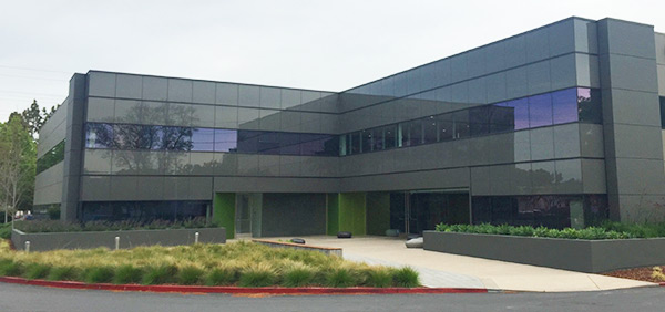
The training is held at Tektronix, Santa Clara, California in US-SCLA Training Room 229. Santa Clara is right in the center of Silicon Valley where many of the important high tech companies in the world are located. For example, Intel, Google, Infinera, Cadence, Cisco, Apple, eBay, Yahoo, and many others are all headquartered in Silicon Valley. In addition, Silicon Valley hosts many companies that are active in photonic integration. The venue address is:
- Tektronix
- US-SCLA-Training Room 229 (2nd Floor)
- 4250 Burton Drive
- Santa Clara CA 95054
Santa Clara is well reachable by car via either San Jose, SJC (12min) or San Francisco, SFO (45 min) airports. For Google directions to Tektronix please click on the map below..

For any questions about the training or logistics, please contact Erik Pennings at erik@7pennies.com or (848) 228-0807.

Silicon Valley attracts a lot of business travelers and for this reason offers a large amount of good hotel accommodations. Given that the training starts early on Monday, we recommend that you arrive on (or before) Sunday evening. And on Friday, the training ends at 3pm PDT so as to allow participants to travel back home on Friday evening.
For a good overview of pricing, ratings, and locations of hotels around Tektronix, please use this Expedia link or this Booking.com link.
For a short list of nearby hotels with good ratings and reasonable prices (in the say $100 to $150 per night range), please check out the following:
- Clarion Inn Silicon Valley 3200 Monterey Road, San Jose CA 95111 408 972 2200. 18 minutes by car. www.clarioninnsiliconvalley.com
- Driftwood 3477 El Camino Real, Santa Clara CA 95051 408 984 3364. 3 minutes by car. www.driftwoodsiliconvalley.com
- Quality Inn & Suites Silicon Valley 2930 El Camino Real, Santa Clara CA 95051 855-239-9223. 8 minutes by car. www.qualityinnsantaclara.com
- Town House Motel San Jose 475 S 2nd St, San Jose CA 95113 800-491-6126. 14 minutes by car. townhousemotelsanjose.com
PIC ARCHIVE
For more info, please check out the archived earlier photonic integration events. Material for these events has been posted and is available on request.